
The focus of our research is on nanoscale electronic and photonic materials and devices, which is at the intersection of electrical engineering, physics, and materials science. The main emphasis is on fundamental research in the physical sciences and engineering that will set the foundations of new materials and device technologies in the future. Recently, we have been working on the following research areas:
Transparent, conductive, and flexible electrodes based on carbon nanotubes and graphene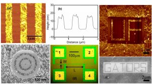
Carbon nanomaterials, such as carbon nanotube (CNT) films and graphene exhibit good electrical conductivity, high optical transparency, and mechanical flexibility. As a result, they are excellent candidates for next generation transparent, conductive, and flexible electrodes for applications such as touch screens, electronic paper, LEDs, photodetectors, and solar cells. Our work in this area includes:
- Fabrication and characterization of metal-semiconductor-metal (MSM) photodetectors with CNT film metal electrodes on silicon and GaAs substrates
- MSM photodetectors with graphene metal electrodes on silicon substrates (Read sample publication)
- Characterization of CNT film/Silicon and graphene/Silicon Schottky barrier photodetectors
Mixed-dimensional van der Waals Schottky junctions between nanomaterials and conventional semiconductors
 For most device applications of nanomaterials, junctions play a significant role. Mixed-dimensional van der Waals heterojunctions are formed by stacking materials with different dimensionality through non-covalent van der Waals interactions. Heterojunctions between nanomaterials and conventional semiconductors combine the advantages of new nanoscale materials with those of well-established semiconductor technology. As a result, investigating such heterojunctions provides important insights for the future integration of nanomaterials with silicon device technology. Our work in this area includes:
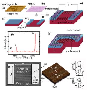
- Graphene/Silicon Schottky junctions with a tunable Schottky barrier height: Investigation of thermionic emission, tunneling, and the Fermi level shift in graphene as function of applied bias
- Investigation of forward-bias diode parameters, electronic noise, and photoresponse of graphene/silicon Schottky junctions with an interfacial native oxide layer
- The electrical properties of CNT film/oxide/Silicon and graphene/oxide/silicon metal-oxide-semiconductor (MOS) devices (Read sample publication)
- Low frequency noise and random telegraph signal (RTS) fluctuations in CNT film/Silicon Schottky junctions (Read sample publication)
Percolation transport in nanostructures
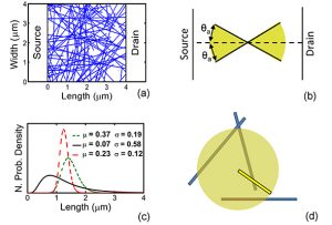 Percolation transport deals with the formation of long-range connectivity in random networks. We have been working on experimental characterization and advanced modeling/simulation of percolation transport in low dimensional nanostructure networks and films. Our work in this area includes:
- Experimental measurement and Monte Carlo simulation of resistivity and 1/f noise scaling in carbon nanotube (CNT) films/networks as a function of nanotube and device parameters (Read sample publication)
- Study of tunneling-percolation conduction in graphene-based multifunctional hybrid nanocomposites
- Investigation of electronic transport in graphene nanoribbon networks/films, such as Mott variable Range Hopping (VRH) and magnetoresistance at low temperatures and high electric fields (Read sample publication)
Controlled growth and heterogeneous integration of nanomaterials with silicon technology
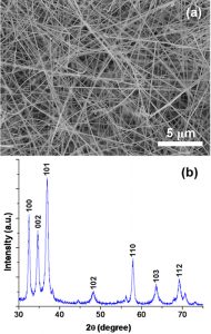
We operate home-made chemical vapor deposition (CVD) systems in our lab for growing a wide range of nanomaterials. Our work in this area includes:
- Advanced methods of nanotube and nanowire growth, such as electric-field aligned growth and plasma enhanced chemical vapor deposition (PECVD) growth
- Ion implanted catalyst for CVD growth of nanotubes and nanowires, such as carbon nanotubes, silicon oxide nanowires, GaN nanowires, and Ga2O3 nanoribbons
- Localized growth of carbon nanotubes on commercial foundry CMOS substrates at room temperature using microheaters fabricated by maskless post-CMOS MEMS processing (Read sample publication)
- Template-assisted growth of nanomaterials, such as nanotubes in porous anodic alumina (PAA) templates
Nanoscale molecular sensors
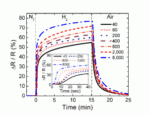 Nanoscale materials have naturally small size, extremely high surface-to-volume ratio, low noise, and low-power consumption. As a result of these significant advantages, they are excellent candidates for molecular gas and vapor sensors. Furthermore, selectivity to different gas molecules can be achieved by surface functionalization. Our work in this are includes:
- Hydrogen sensors using Palladium-coated graphene nanoribbon networks (Read sample publication)
- Platinum functionalized graphene nanoribbon films (GNFs) for ammonia sensing
- Hydrogen sensing with functionalized GaN nanowire devices
- Nanoscale gas sensors for biomedical applications